Key Notes
- SK Hynix is reportedly discussing its first US memory wafer production with Intel, with an Ohio lease and a joint venture among the possibilities.
- The talks remain exploratory, and neither company has announced an agreement or production schedule.
- A fabrication deal would be distinct from SK Hynix’s confirmed Indiana packaging investment and could face South Korean technology review.
SK Hynix is in talks with Intel about manufacturing memory chips in the United States for the first time, according to Reuters, opening a potential route to additional American production as AI infrastructure investment increases demand for memory.
The options include leasing part of Intel’s planned Ohio facility or forming a joint venture involving Intel and major cloud companies, the report said. The discussions are exploratory, and no decision has been made.
A completed agreement could give SK Hynix a domestic manufacturing foothold near American customers while helping Intel find a use for capacity it has been building. Those potential benefits depend on a transaction whose structure, financing and production timetable remain unannounced.
An Ohio Lease Would Differ From a Foundry Order
Reuters cited three people familiar with the discussions. SK Hynix said it was examining options to strengthen its memory business, including additional production bases, but had made no decisions. Intel declined to discuss speculation and said investment in Ohio was continuing.
The distinction between the proposed arrangements is consequential. Leasing factory space would not, by itself, mean SK Hynix had ordered wafers manufactured using Intel’s process technology. A joint venture would introduce different questions about ownership, operating responsibility and how participating customers secure supplies.
For Intel, a partner could help support the economics of a major construction project. It would take disclosed commercial terms to establish how much revenue, capital relief or manufacturing work the company would receive.
Intel Has Linked Expansion to Customer Demand
Ohio has already illustrated the difficulty of matching semiconductor construction to future business. In a February 2025 update, Intel said it planned to complete its first Ohio fab in 2030, with operations beginning in 2030 or 2031. Those were company targets, not a start date for any SK Hynix operation.
Chief Executive Lip-Bu Tan subsequently told employees in July 2025 that Intel was slowing Ohio construction further to align spending with demand, while retaining flexibility to accelerate if it won customers.
That policy provides context for why a possible memory partnership matters. Customer participation could give the project a more concrete source of demand, but the reported negotiations do not establish that construction will accelerate or that an existing schedule has changed.
Indiana Packaging Is Already a Separate Commitment
SK Hynix already has a confirmed American investment, but it serves a different stage of production. The company held a groundbreaking ceremony in Indiana on August 27 for an advanced packaging facility intended to supply next-generation high-bandwidth memory, or HBM.
Its announcement describes an investment exceeding $4 billion, a cleanroom opening targeted for October 2028 and mass production planned for the second half of 2029. Wafers manufactured in South Korea would be sent to Indiana for packaging and testing.
Domestic wafer fabrication would therefore add a different capability from the Indiana project. Producing the memory circuits and assembling those circuits into finished packages are separate parts of the supply chain; announcing one does not mean both are already available in the United States.
The Indiana plans also include an advanced packaging research and development testbed. That commitment shows the company’s interest in working close to customers and research partners, independently of whether the Intel discussions produce an agreement.
AI Demand Creates an Opening, With Conditions Attached
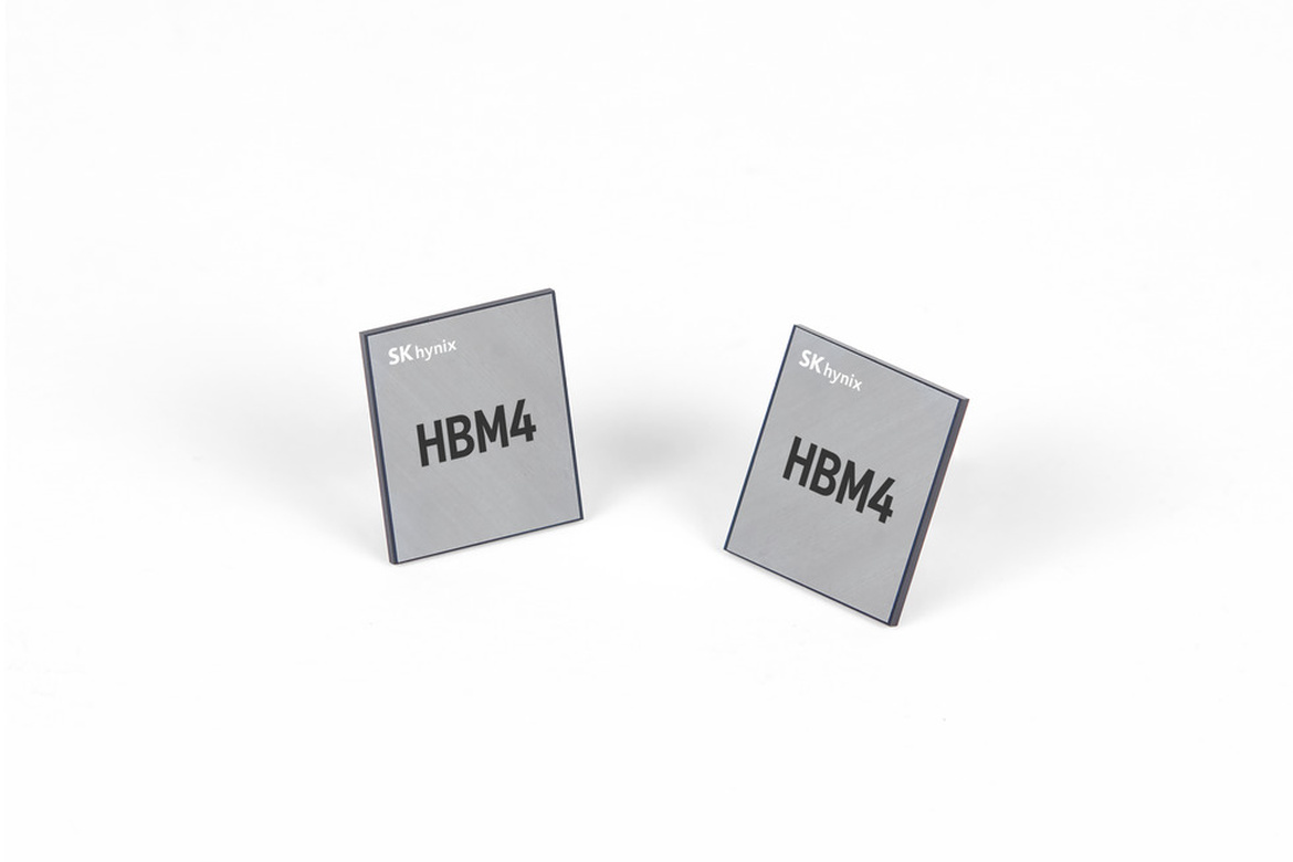
HBM stacks multiple DRAM chips to move large amounts of data efficiently, making memory performance central to the AI accelerator market. SK Hynix has identified bandwidth and power efficiency as priorities in its HBM4 development.
The memory boom has also benefited competitors, including Samsung. For customers considering a manufacturing partnership, securing future supply could matter alongside the purchase price of individual chips.
South Korean technology rules remain a potential constraint. Reuters reported that advanced memory production abroad could face government scrutiny; the trade ministry said projects involving national core technology would require review under the Industrial Technology Protection Act.
That is a possible approval requirement, not an announced rejection. The product mix, technology involved and final transaction structure would matter to any assessment.
Following recent volatility in SK Hynix shares, the key distinction for investors is between discussions and commitments. A signed agreement would need to clarify investment obligations, customer participation and the path to production before the proposed capacity could be counted on to ease supply constraints.