Key Notes
- TSMC is reportedly exploring 3D DRAM production at Nvidia’s request, with no disclosed timetable for manufacturing.
- The technology concerns vertically arranged memory cells, a different concept from stacking separate DRAM dies into HBM packages.
- TSMC’s latest quarter delivered $46.72 billion in revenue and a 66.4% gross margin, setting a demanding benchmark for new investment.
Nvidia Corp. (Nasdaq: NVDA) has asked TSMC (NYSE: TSM) to explore 3D DRAM production, The Information reported Friday.
The potential expansion would bring the world’s largest contract chipmaker further into the memory business as AI demand strains supply. Reuters, citing the report, said TSMC is considering building new facilities or acquiring and converting an existing plant. A production timetable was not disclosed, and neither company immediately responded to the news agency’s requests for comment.
TSMC’s US-listed depositary shares were trading at $374.17, up 6.0%, at approximately 12:17 p.m. Eastern time, or 17:17 UTC, on November 6. Nvidia was up 3.5% at $187.94. Both participated in a broader chip-stock recovery after Thursday’s selloff.
Memory Becomes a Constraint on AI Growth
For Nvidia, access to memory helps determine how many complete AI systems it can deliver. Manufacturing more processors does not solve a shortage of the components needed to feed them data. High-bandwidth memory supplies that data close to the GPU, while other forms of DRAM support the CPUs and wider server system.
Supply constraints were already affecting product choices months before Friday’s report. In a June 10 assessment, TrendForce said Nvidia had reduced the SOCAMM memory configuration of its Vera Rubin Superchip modules because of insufficient low-power DRAM allocations in suppliers’ preliminary 2027 production plans.
The research firm estimated at the time that those allocations would cover only about 60% of Nvidia’s projected requirements. That was a forward estimate about low-power DRAM, not a measurement of today’s entire memory market. It nevertheless showed how component availability could force the company to change a system’s configuration even while demand remained strong.
3D DRAM Changes the Memory Cell, Not Just the Package
DRAM temporarily holds data while a computer works on it. The 3D approach described in the report builds memory cells vertically to fit more storage into a given area, extending capacity beyond what can be achieved by arranging cells in a single horizontal layer.
That is a different manufacturing concept from the stacking already used in HBM. Today’s HBM packages place multiple DRAM dies on top of one another and connect them through vertical interconnects. The reported 3D DRAM initiative concerns the structure of the memory cells within the chips.
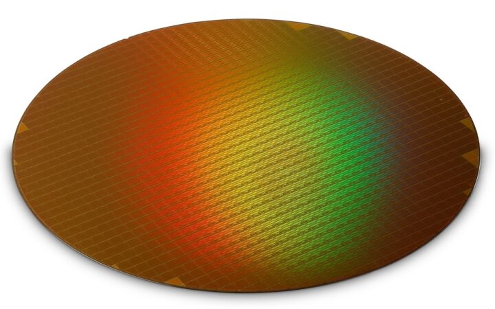
Higher density could increase the memory capacity produced from a wafer. The payoff would depend on production yield, processing costs and whether customers qualify the chips for their systems. No capacity target or manufacturing schedule was disclosed in the news account.
TSMC Already Has a Role in HBM Development
TSMC’s relationship with the memory industry is not starting from scratch. SK hynix (KRX: 000660) announced an agreement in April 2024 to collaborate on HBM4 development and advanced packaging.
That agreement called for TSMC’s advanced logic process to be used for HBM4’s base die, which sits beneath the memory stack. It also covered closer integration with TSMC’s CoWoS packaging technology. Manufacturing the logic underneath a memory stack and manufacturing the DRAM cells that store its data involve different parts of the production chain.
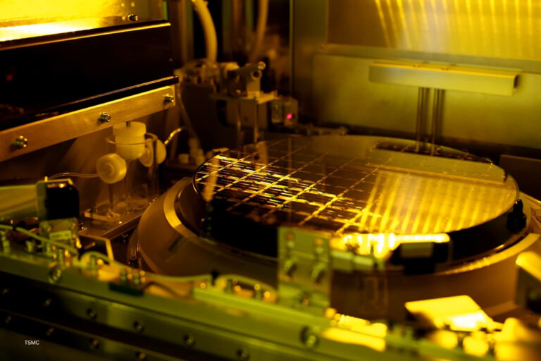
Nvidia and TSMC have also deepened cooperation inside the fab. In May, Nvidia outlined work spanning computational lithography, process simulation, production scheduling and defect inspection. TSMC is using Nvidia’s AI technology to identify tiny wafer defects and improve factory operations, work that reaches directly into the cost and reliability of chip production.
A New Business Would Face a High Profitability Bar
TSMC enters the discussion with a highly profitable existing business. Its October 15 results showed third-quarter revenue of $46.72 billion, up 41.2% in US-dollar terms, and a gross margin of 66.4%. The final release followed the record sales evident in its monthly disclosures.
A memory expansion would require its own spending plan and return targets. A new fab ties up capital before shipments generate cash, while converting an existing facility still requires equipment, process development and customer qualification. Production yield—the proportion of output that meets specifications—would help determine the cost of each usable chip.
The first financial sign of a larger commitment would be a disclosed site, capital budget and qualification timetable. Those details would turn Nvidia’s reported request into manufacturing capacity that shareholders could begin to model.